

The use of self-organization phenomena at semiconducting surfaces allows fabricating quantum dot structures for producing novel nanodevices with unprecedented applications not only in optoelectronics, but also for room temperature operating single electron transistors and/or resonant tunneling structures. Fabrication of ultra-dense Ge dots on silicon surfaces still presents a series of problems far to be completly manageable, thus limiting their density to values between 109 and 1010 cm-2. Ge islands growth on SiO2 films, occurring through a Volmer-Weber mechanism, allows well higher dots density. This work present the growth of crystalline Ge nanostructures with average dot size of (5 ± 1) nm and very high dot density of about 2.8 x 1012 cm-2. Ge dots appear almost flat with a beginning of faceting and characterized by a low aspect ratio. Furthermore from the I-V curves we measured an energy gap of about 1.8 eV that is well wider than that of Ge bulk thus indicating the occurrence of a quantum confinement effect. After SiO2 3.0 nm thick film cleaning, growth of Ge dots have been obtained by following a two steps process. First, four monolayers (MLs) of Ge have been deposited on the SiO2 clean surface kept at room temperature (RT), then the sample has been in-situ annealed at 500oC for 30 minutes. The STM image of the clean SiO2 surface nicely mimics the shape of Si(001) underneath surface resulting in a perfect sequence of terraces 70 nm wide and monoatomic steps with a roughness of 0.06 nm (shown in Figure 1 a)). On terraces we observed small isolated white spots, with a density of about 1×1013 cm-2, forming a highly defected substrate. After 4 ML Ge deposition at room temperature, the STM image showed a complete coverage of the SiO2 surface and randomly distributed, strictly interconnected Ge amorphous clusters with a density of about 3.8 x 1012 cm-2 ( shown in Fig.1 b)). The subsequent heating at 500oC changed the surface morphology giving rise to individually separated Ge dots, with a density of 2.8×1012 cm-2 (Figure 1 c)). The Ge dots average lateral size is (5 ± 1) nm. Statistical analysis, carried out on more than one hundred islands, leads to an aspect ratio of (0.17±0.04), a value lower than all those reported in literature for similar coverages.
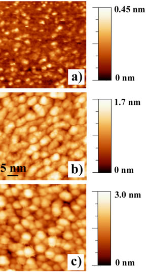
Figure 1
Figure 1- a) STM image of the SiO2 substrate. Vsample = -3.0 V, I = 0.5 nA b) STM image of 4 MLs of Ge deposited on SiO2/Si(001) surface kept at room temperature. V sample = 2.0 V, I = 1.0 nA; c) STM image of the sample shown in the panel b) after annealing at 500oC for 30 min. V sample =3.0 V, I = 0.5 nA. Gray-scale ranges (at left) confirm the sizeable changes in the RMS roughness values passing from the bare SiO2 substrate to the amorphous deposited Ge film and the Ge dots.
An important point of debate is the shape of these dots, generally reported to be hemispherical. By making a careful study based on the surface gradient analysis of the shape of the Ge dots we found that they appear almost flat with beginning of faceting along the {113} planes. Interestingly, the Ge dots are completely not oxidized after the heating procedure as measured by the XPS spectra. This also suggests that no bonds involving Ge atoms and SiO2 substrate are formed at the interface. On the other hand, it is worth noting that the total volume of Ge dots is approximately the same than the volume of the deposited Ge layers. This means that there is neither formation of a wetting layer, nor Ge atoms desorption during the thermal treatment, nor intermixing between Si and Ge atoms. These XPS results, as well as those of the surface gradient analysis, indicate that SiO2 film always isolates Ge dots from the Si bare substrate. Another interesting aspect to investigate is the electronic behaviour of these nanostructures. The I-V and the conductance curves recorded on the Ge dots have been compared to that obtained for a Ge nominal deposition of 5 MLs characterized by Ge dots with an average lateral size of about 50 nm. Our results show that by reducing the cluster size, there is a significant reduction of the conductance thus meaning that the energy bandgap increases from approximately 0.7 eV to 1.8 eV. This is a hint that energy bandgap widening is an intrinsic property of the Ge dots induced by quantum confinement that changes significantly their electronic band structure.
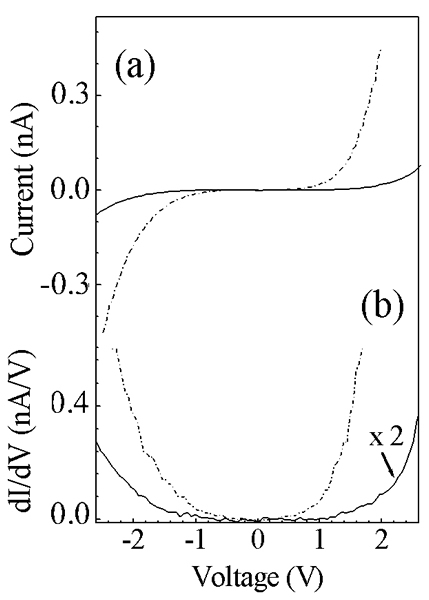
Figure 2
Figure 2 – I-V (a) and conductance (b) curves for the 4 MLs of Ge deposited on SiO2/Si(001) surface kept at room temperature and annealed at 500oC for 30 minutes (solid lines) and for a 35 MLs nominal Ge deposition (dot dashed lines).
The direct measurement of this gap is important because it can be related to the room temperature photoluminescence (PL) feature observed in case of Ge dots. This PL signal has been generally observed for Ge dots embedded or deposited on SiO2 and in the past was interpreted as due to recombination through radiative states at the Ge/SiO2 interfaces. Our I-V measurement pointed out that the PL peak can be not only attributed to the recombination through radiative states at the Ge/SiO2 interfaces but also to a genuine quantum confinement effect. In conclusion, isolated, almost flat, nonepitaxial and not oxidised Ge dots with an average lateral size of approximately 5 nm, a low aspect ratio and a density of 2.8 x 1012 cm-2 have been grown. They show a semiconducting behaviour with a value of the energy gap well wider than that of Ge bulk, to be ascribed to their reduced size. The high density together with the observation of the widening of the energy gap makes the Ge islands on SiO2 very promising for application in optoelectronics.
Reference
I. Berbezier, A. Karmous, A. Ronda, A. Sgarlata, A. Balzarotti, P. Castrucci, M. Scarselli, M. De Crescenzi, Applied Physics Letters 89, 063122 (2006) paper selected to appear on Virtual Journal of Nanoscale Science & Technology, Volume 14, issue 9, (2006)
Experimental team
A. Sgarlata, A. Balzarotti, P. Castrucci, M. Scarselli, M. De Crescenzi , NAST Centre
I. Berbezier, A. Karmous, A. Ronda, L2MP UMR CNRS 6137, Polytech Marseille-Technopole de Château Gombert, 13451 Marseille, France
Related Information
Prof. M. De Crescenzi
Virtual Journal of Nanoscale Science & Technology