

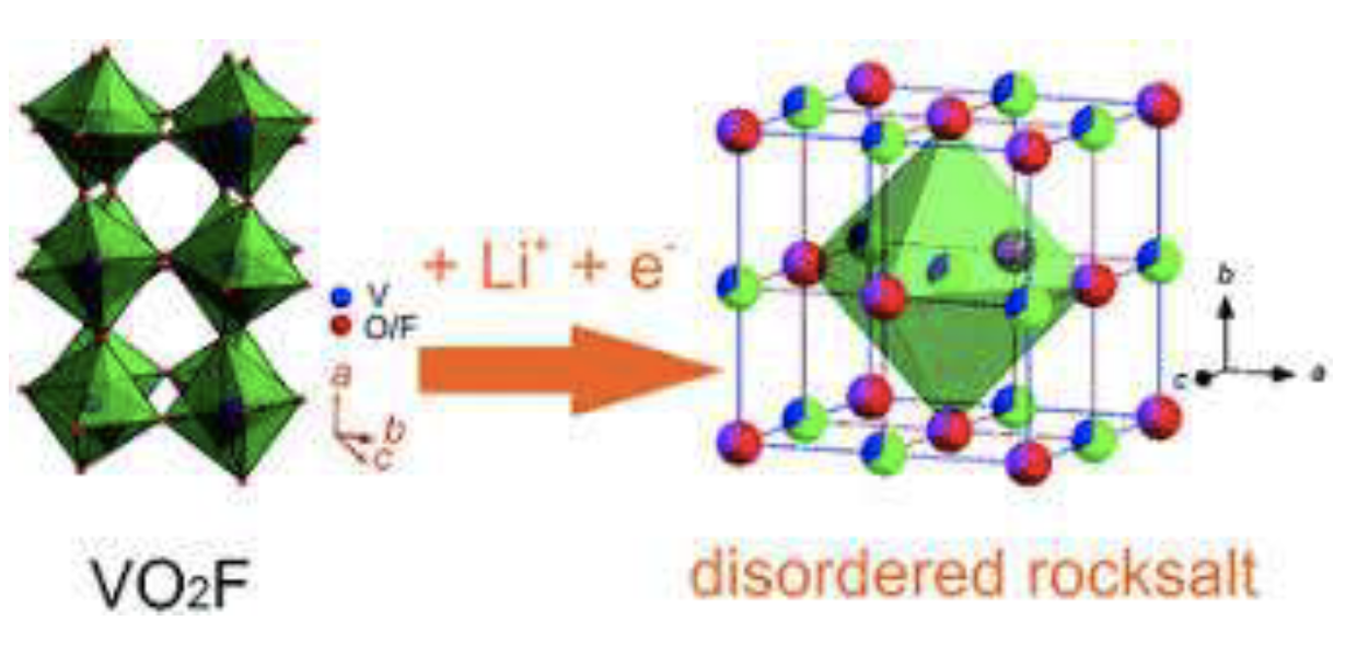
A selection of research activities with potential impact in Energy
Physical Characterization
Access to skills and tools for the characterization of macroscopic and microscopic physical properties of composite materials: microsocpic structure and imaging of materials from the micron to the atomic scale, characterization of surface roughness, absorption and emission properties of electromagnetic radiation, both surface that of volume. Instrumentation available for characterizations:
- X-ray reflectometer and dispersion diffractometer (also angular) for: a) determination of thickness and roughness of thin film surface / interface; b) analysis of the crystalline phases and the degree of crystallinity of the materials; c) real-time monitoring of compound formation; d) structure of composite materials; e) identification of crystalline phases in materials.
- Confocal Micro Raman Spectrometer / TERS – for high resolution 2D and 3D maps for the chemical-physical analysis of films and multilayers – integrated with AFM microscope.
- Scanning probe microscopes (AFM, STM) to characterize morphological, nanomechanical, electronic and optical properties of materials with sub-nanometric resolution.
- Spectrometers for time-resolved optical spectroscopy measurements, to characterize dynamic charge carriers in materials
- Differential Scanning Calorimeter (DSC) to measure characteristic thermal transitions of materials
- Thermogravimetry (TGA) for analysis of the thermal stability of materials
- Ellipsometer for the characterization of the thicknesses and surface properties of structures at the micron scale
- Fluorescence X spectrometer combined with Raman spectroscopy and high resolution gamma spectroscopy
- High vacuum scanning electron microscope (Cambridge S200) with integrated STM and laser access for tip-enhanced laser nanostructures
- Variable pressure electronic microscope (TESCAN VEGA3) with integrated ultra-flat AFM
Access to skills, instruments and technologies for the characterization of chemical-physical properties and chemical analysis of materials, qualitative and quantitative analysis of components and solutes and for analysis of volatile substances, spectroscopic analysis of compounds, morphological analysis with electron microscopy, NMR spectroscopy for characterization of organic molecules and biological macromolecules:
- GC-IMS; ion mobility detector with chromatographic separation
- GC / MS double column
- ATR-FTIR
- Homo and heteronuclear high resolution magnetic resonance (NMR) (400 and 700 MHz)
- Scanning electron microscope with high vacuum EDS for morphological and chemical analysis of materials
Electronic and optoelectronic characterization for composite materials
Measurement of the transport properties of materials. Different measurement techniques of electrical and electronic properties will be made available: I-V, C-V characterizations, surface and volume resistivity measurements, photoconductivity and spectral photoemission, as well as the dielectric constant of the insulating materials and the modulus of elasticity:
- Impedance spectroscopy
- Frequency analysis
- Measurements of photoconductance maps and LBIC maps
- Thermoelectric measurements
- Characterization under solar simulator in both static and dynamic conditions
- Benchtop FE / SEM for fast analysis of devices and samples
Sample and device preparation
User access to skills, equipments and technologies for design, preparation and construction of devices – to be characterized (with the instrumentation of ISIS@MACH and with the ISIS neutron and muon beamlines – and samples to be prepared for the specific characterizetion – e.g. metallization of samples for SEM analysis, electrical contacting of devices, assembly of samples for spectroscopic and AFM analysis, microfabrication and laser ablation:
- characterization of transistors and microelectronic devices (High frequency electronics and electronics at high integration VLSI)
- electronic and optical properties of semiconductor nanostructures
- Fully equipped chemical laboratories for synthesis
- Multihead ink-jet printer, 3D printer
- Precision mechanical instrumentation for bench for the micromechanical realization of devices
- Pulsed Laser Deposition (NIR, VIS, UV)
- Subpicosecond infrared laser for micromachining, marking, evaporation
- Sputtering and thermal evaporator for metals
- Ultrasonic disintegrator