

The idea that bottom up nanofabrication can be achieved by the joint use of nanometrically controlled sharp tips and electromagnetic radiation. If we think of an irradiated STM tip as an electromagnetic antenna operating at optical rather than radio frequencies, we can understand how, in the vicinity of its highly curved apex, extremely high electromagnetic field intensities can be achieved. This well known fact is at the base of the so called “Surface” Enhanced Raman Spectroscopy, where the field enhancement is in fact due to nanometric corrugations of the surfaces; but it can also be exploited to bring the high intensity e.m. field where we want by a piezo controlled nanometric tip. Such intense radiation can be used for all the purposes for which we use lasers in the macro world: ablation, melting, recrystallization, welding, photoionization, spectroscopy and spectroscopic imaging. There are several advantages in this: the most obvious is that in the near field of the tip we can obtain concentrated radiation in a region smaller than the diffraction limit; more easily, we can obtain radiation effects in regions smaller 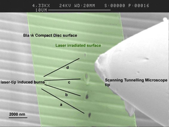 than the practically used focal volumes, which are often hundreds of microns wide. As a secondary advantage, we can deliberately increase the focal region in order to obtain a smaller dependence on the alignment precision, on vibrations, on thermal effects, still retaining nanometric resolution. The other obvious advantage is the ability to subtract or add material from a surface at the nano scale, and characterize what we have done, both morphologically and spectroscopically, in real time by the same apparatus. In the following figures we report an example of holes burnt in an optical Compact Disk by mildly focussed laser radiation impinging on a STM tip, as imaged by Scanning Electron Microscopy; and different examples of spatially resolved depositions of both biological (the aminoacid tryptophan) and metallic (lead) material on flat surfaces as imaged by AFM and STM.
Burns onto a blank CD surface are produced by laser pulses at 540 nm, irradiating the surface at very low angle, when the STM tip is brought close to the tunnelling distance. The laser beam is mildly focussed by a 500 mm focal length lens so that the beamwaist is of the order of 102 microns, much wider than the burns size, as evidenced by the green shaded area.
 A deposition of the aminoacid tryptophan is obtained by photoionizing gas phase neutral molecules, as vaporized from a solid sample, under a micrometric electrode positioned 20 microns above the surface. The laser beam size is again of the order of 102 μm, while the deposition, as imaged by AFM here, is 20 μm.
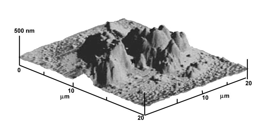
Exploiting the narrow resonant excitation of the first excited electronic state of lead we can photoionize laser ablated atoms and pin them down on the underlying surface by an applied electric field. Real time STM imaging shows that the spot size depends on the tip-surface distance. Rastering the tip over the surface produces a square deposition of photoionized atoms.
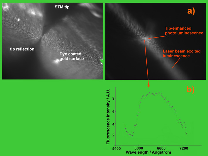
The next figure shows an optical microscopy view of the tip-enhancement of the fluorescence excitation as measured on a layer of the organic dye Rhodamine 6G.
The spectral distribution of the photoluminescence collected from the most luminous spot under the tip ensures that the dye molecules are not damaged. This technique thus ensures the ability to characterize spectroscopically micro-nano selected regions.
| Related Information Dr. P. Morales ENEA |