

 3th April 2007 – 15:00
Speaker:
Prof. Maurizio De Crescenzi (Università degli Studi di Roma Tor Vergata)
Location:
U.M. Grassano, Campus
Abstract:
Photovoltaic effect has always relied on semiconductors p-n junctions based on doped silicon or III-V-semiconductors. Recently, however, the use of carbon nanotubes has evoked large promises to increase the potential of light conversion and current generation (1). Carbon nanotubes in fact possess extended π-electron systems and characteristic van Hove singularities, which in combination with photoexcitable electron donors can provide the basic structural element for efficient photovoltaic conversion devices as demonstrated by Lee et al. (2) and by Guldi et al. (3). However single wall carbon nanotubes (SWCNTs) have shown a low efficiency (0.2%). Relative to SWCNTs, multi wall carbon nanotubes (MWCNTs) present a number of important applicative advantages. In particular, they are slightly easier to process than SWCNTs, because they generally do not form bundles and are found to be straight. Moreover, due the large number of concentric graphitic inner shells, they appear more suitable for achieving charge transfer and charge transport. Remarkably, also MWCNTs can be good light converters as shown by our own recent measurements reported in Ref. (4). We have demonstrated in fact the ability of multi wall carbon nanotubes to generate photocurrent upon the whole visible and ultraviolet spectral range.
Photocurrent measurement of MWNTs/SiO2 electrode, put in an electrochemical cell, was excited with visible light and a solution of 0.5 M NaI and 0.01M I2 in acetonitrile has been used as electrolite. The maximum photon-to-current conversion efficiency is approximately 7%, about 50 times higher than that reported for single wall carbon nanotubes.
Our experience shows that the lifetimes of the charge separated species are enough long to consider nanotubes excellent candidates for the fabrication of photovoltaic nanodevices and solar energy conversion applications.
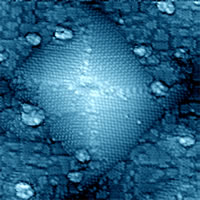
Photocurrent generation of nanometric Ge droplets has been also investigated by using the same electrochemical photocurrent apparatus. Ge dots have been grown depositing by MBE several nominal thicknesses of Ge (ranging from 0.5 to 15 nm) on clean SiO2 surface at room temperature and then annealed to reach full crystallization. The photocurrent signals always show a feature located at about 280 nm. This peak can be ascribed to the bulk direct electronic transitions located at X point of the Brillouin zone. Only in the case of 0.5 nm Ge film a broad and intense feature at 550 nm has been observed while the peak due to the bulk direct electronic transitions results to be dramatically reduced. Since this last sample is characterized by 5 nm nanodots medium size (the smallest among the measured samples) this broad band in the photocurrent can be due to quantum confinement effect. On the other hand we have already reported for this sample a significant increase of the energy band gap to approximately to 1.8 eV from STM I-V measurements (5). This means that only for very small quantum dots an efficient electron-hole separation occurs thus generating a significant photocurrent in the visible range. This result is of particular relevance for photovoltaic nanodevices and quantum dot based lasers.
(1) S.Barazzouk, S. Hotchandani, K. Vinodgopal, P. V. Kamat, J. Phys. Chem. B 108, 17015 (2004).
(2) J.U. Lee, Appl. Phys. Lett. 87, 073101 (2005).
(3) D.M.Guldi, G.M.A.Rahman, M.Prato, N.J.Jux, S.Qin, W.Ford, Angew.Chem.Int.Ed.44, 2015 (2005).
(4) P.Castrucci, F. Tombolini, M. Scarselli, E. Speiser, S. Del Gobbo, W. Richter, M.Diociaiuti,
M. De Crescenzi, Appl. Phys. Lett. 89, 253107 (2006).
(5) I.Berbezier, A. Karmous, A. Ronda, A. Sgarlata, A. Balzarotti, P. Castrucci, M. Scarselli,
M. De Crescenzi, Appl.Phys.Lett.89, 063122 (2006).
Related Information:
Nano Phd School
Università degli Studi di Roma Tor Vergata