

Spider fibers are an exceptionally resistant material based on the fibroin protein. The most obviuous property of spider fibers is however that they can be meters long but they are micro- or even nanometric in their cross section. This makes it relatively easy and inexpensive to manipulate the fibers and exploit their nanometric size properties. Furthermore, in spite of their sizes, due to their non uniform density, spider silks are efficient scatterers of visible radiation, which makes them easily observable with inexpensive equipment, contributing to the ease of manipulation. Fibers are often composed of fibrils that can be as thin as a few tens of nm, reaching thus the range of sizes of other natural exploitable nanoobjects such as rod type or filamentous and bacteriophage viruses.
After separating such fibrils from the bundle, The NAST Center team in collaboration with the ENEA Casaccia Surface Science laboratory used them for two simple nanotechnological applications: 1) as shadow masks to obtain extremely small and controllable nanogaps separating metal electrodes; 2) as a mechanical support to produce metallic micro- and nanowires.
Insulating gaps as narrow as 15 nm were obtained between gold electrodes over distances in the range of 10-3 or even 10-2 m. Gold was thermally evaporated on nanofibers, stretched across a slightly curved mica slab in order to obain a good adhesion; by rotation of the slab around an axis nearly corresponding to the adhering fiber, the designed shadow was made much smaller than the fiber itself.
Figure 1 shows an AFM topographic image of such electrodes obtained on stretching three fibers of
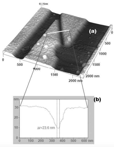
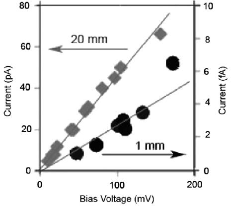
Figure 1. 600 nm, 250 nm and 15-20 Figure 2 The electrical conduction
nm wide gaps ina gold layer obtained characteristics of 20 mm long
by shadowing with spider silks gap vs those of 1 mm long gap, in air
different sizes, while figure 2 shows the lower insulating properties of a 2 cm long gap with respect to a 1 mm long gap.
Fibers were also gold coated uniformly all around by means of a suitable holder and their electrical conduction was probed. Figure 3 shows a linear, ohmic behaviour, which is maintained by slightly stretching the wire, while it drops to zero when stretched by more than 2% of it length.
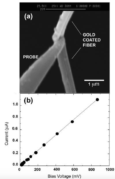
Figure 3 . a) shows an SEM image of a double gold coated 350 nm
diameter spider fiber stretched by a nanomanipulated Scanning Probe
tip in the SEM vacuum chamber;
- b) shows the linear, ohmic behabviour of the current vs bias before the fiber breaks due to the stretching action
The ease of manipulation of spider fibers and the negligible cost of fabrication of nano-gaps and wires makes this method extremely useful for the straightforward assemblage and electrical connection of experimental microdevices, such as in the development and testing of lab-on-the-chip type 3D systems.
The full article can be accessed electronically at www.iopscience.iop.org (Nanotechnology, Volume 23, Issue Number 25, 255304)
Authors from NAST Centre: Mario Caruso, Davide Flammini, Piero Morales
Other Contributors: Bruno Rapone and Piero Morales