

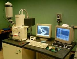
LEO 35 Field Emission by Zeiss©
Characteristics
• GEMINI® based Field emission e-beam column capable of ultra high resolution SEM up to 25 KV.
• Achieves a similar low energy spread compared to a cold field emission source, but with a much higher emission current and much higher beam stability.
• Featuring a TV camera and three detectors, i.e. (i) secondary electrons detector, (ii) back-scatter electrons detector (EBSD) , (iii) In-lens detector for ultra high resolution imaging (<10nm).
• Equipped with an energy dispersive x-Ray spectrometer (EDS) from Oxford INCA© allowing for acquisition of sample emitted x-rays. Accompanying software with embedded database of reference spectra for elements identification/recognition, compositional nano-analysis and x-ray mapping.
• Automated stage controlled by a joystick with x-y-z translations, z rotation (full 360° range) and x tilting (up to 90° tilt) for ultra high precision sample positioning.
• Vacuum system (a rotary pump plus a turbo pump) to achieve chamber vacuum of less than 2 x 10⁻⁶ mbar.
• Dynamic vibration-damper.
• Several stubs settings and adaptors for mounting samples on the stage.
• Sample preparation desk.
• Sputter-coater to metallize non-conductive samples (with gold or other target).
Some Results
SEM is a common tool to address a variety of aspects in material research and nanotechnology. For illustrative purposes, some examples of SEM work in a variety of research areas (e.g energy, environment, biotechnology and nanotechnology in general) are reported here. As far as energy and environment are concerned, ceramics and nanostructured materials are key in applications such as fuel cells and chemical sensors. Fig.1 shows a surface micrograph of a composite porous electrode (cathode) designed for Solid Oxide Fuel Cell applications and fabricated by Pulsed Laser Deposition technique. Pd-Au metal droplets have been deposited and condensed on a continuous open La0.8Sr0.2Co0.8Fe0.2O3-δ network, previously grown on a dense polycrystalline stabilized ZrO2. Mixed ionic and electronic properties of La0.8Sr0.2Co0.8Fe0.2O3-δ assisted by the electrical properties of metal droplets at high temperature, reduce the cathode polarization in SOFCs.
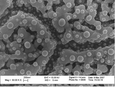
Figure 1
Figure 1. Surface of a composite porous electrode (cathode) designed for SOFC applications and fabricated by Pulsed Laser Deposition technique. Pd-Au metal droplets were deposited onto a continuous open La0.8Sr0.2Co0.8Fe0.2O3-δ network grown on dense polycrystalline stabilized ZrO2.
Another class of fuel cells are based on the usage of polymeric “Proton Exchange Membranes” (PEM) as the fuel cell electrolyte. Nafion is the best performing polymer currently available for this application but, amongst other drawbacks, suffers of a marked drop in conductivity for working temperatures above 90°C due to morphological transitional and de-hydration. A variety of composite membrane, i.e. hybrid structures of Nafion with dispersed fillers, are under investigation to overcome this problem. Figure 2 shows an example of Nafion mixed with an inorganic phase “sulfonate diphenyl silane diol” (SDPSD), appearing as “bright” islands in the photos. The PEM performances improve based on the content and distribution of the SDPSD. Thermal treatment is one way of controlling the microstructure of the composite structure. SEM micrographs clearly shows that heating the samples at 170 °C induces a finer dispersion of the filler, yielding more minute SDPSD clusters. The limited electronic conductivity of this material makes it difficult to analyze with the SEM.
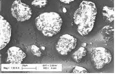
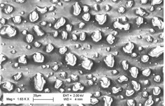
Figure 2. Two SEM pictures of theNafion/SDPSD 70:30 composite membrane for PEM fuel cells. Photos selected demonstrate the effect of the thermal treatment at 170°C on the dispersion SDPSD in the microstructure. Sample “as-prepared” (far left) and the “heat-treated” one (left) exhibit different dispersion of SDPSD islands within the Nafion matrix, highlighting a size reduction of the SDPSD clusters induced by the thermal treatment.
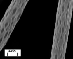
Figure 3
SEM imaging is also crucial for the characterization of nanostructured materials for biological applications. Within biotechnology, tissue engineering combines the fields of engineering, chemistry, biology, and medicine to fabricate replacement tissues able to restore, maintain, or improve structurally and functionally damaged organs. Polymeric scaffolds for stem cells growth and differentiation represent an active research topic. Some scaffolds are fabricated by electrospinning as highly interconnected porous polymeric networks. Figure 3 shows a SEM image of nanostructured PLA electrospun nanofibers endowed with nanopores. Such fibres are multiscale features, having lengths in the centimetre range, micrometric and sub-micrometric diameters and nanoscale roughness/porosity. The various length-scales can be largely tuned and tailored through processing parameters.
Figure 3. SEM image of PLA electrospun nanofibers with nanopores. The fibres have a multiscale geometry with lengths in the centimetre range, diameters between few tens of nanometers and few micrometers, and nanoscale porosity. Length-scales can be tuned and tailored through processing parameters. Controlled porosity is important also for drug delivery.
The topics briefly highlighted in the examples are discussed in greater details in several papers. The interested reader can consult the selected papers cited in the reference.
SEM capabilities go beyond pure geometrical and morphological information, highlighted in the previous examples. In fact backscattered electrons and EDS can be used to obtain compositional data. In the next example in Figure 4, a carbon nanoparticle of about 400 nm deposited from the environment onto a substrate made of nanoporous Si. The X-ray spectra shown on the left were collected with the EDS at two different locations pointed out in the SEM micrograph, i.e. at point (1) centered on the nanoparticle and at point (2) away from it. From comparison, the missing peak in the spectrum collected at site (2) is characteristic of C, which reveals the chemical nature of the nanoparticle.
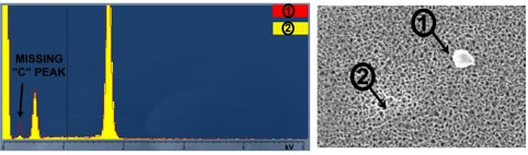 Figure 4: Micro-analisys by EDS of a 400nm carbon particle (site 1) deposited from the environment onto a nanoporous Si substrate. The nature of the nanoparticle is highlighted as a “difference”, because the yellow spectrum at site (2) is missing a peak characteristic of carbon and present in the red spectrum at site (1).
References on SOFC and PEM
[1] D. Z. de Florio, R. Muccillo, V. Esposito, E. Di Bartolomeo and E. Traversa, “Preparation and Electrochemical Characterization of Perovskite/YSZ Ceramic Films”, J. Electrochem. Soc., 152 (1), A88, (2005).
[2] V. Esposito, D. Z. de Florio, F.C. Fonseca, E.N.S. Muccillo, R. Muccillo and E. Traversa, “Electrical properties of YSZ/NiO composites prepared by a liquid mixture technique”, J. Eur. Ceram. Soc., 25, 2637, (2005).
[3] Deganello, V. Esposito, E. Traversa and M. Miyayama. “Cathode performance of nostructured La1-aSraCo1-bFebO3-d on a Ce0.8Sm0.2O2 electrolyte prepared by citrate-nitrate auto-combustion”, F J. Electrochem. Soc., 154 (2), A89, (2007).
[4] Barbara Mecheri, Alessandra D’Epifanio, Enrico Traversa, Silvia Licoccia. “Effect of an ormosil-based filler on the physico-chemical and electrochemical properties of Nafion membranes”, J. Power Sources, 169 (2007) 247–252.
References on Chemical Sensors
[5] M.L. Grilli, E. Di Bartolomeo, A. Lunardi, L. Chevallier, S. Cordiner and E. Traversa, “Planar Non-Nernstian electrochemical sensors: field test in the exhaust of a spark ignition engine”. Sensors and Actuators B, 108 (2005) 319-325
[6] L. Chevallier, M.L. Grilli, E. Di Bartolomeo and E. Traversa. “Non-Nernstian planar sensors based on YSZ with Ta (10 at.%)-doped nanosized titania as sensing electrode for high temperature applications”. International Journal of Applied Ceramic Technology, 3 [5] 393-400 (2006)
References on Tissue Engineering
[7] E. Traversa, B. Mecheri, C. Mandoli, S. Soliman, A. Rinaldi, S. Licoccia, G. Forte, F. Pagliari, S. Pagliari, F. Carotenuto, M. Minieri, P. Di Nardo. “Tuning Hierarchical Architecture of 3D Polymeric Scaffolds for Cardiac Tissue Engineering”, J. Exp. Nanoscience, (accepted sept. 2007).
Related Information
contact: Prof. E. Traversa; Dr. A. Rinaldi