

A home made piezoscanner, designed for xy scanning of the sample, is hosted on the sample stage of a modified Cambridge S200 scanning electron microscope, while the STM tip is positioned on the desired feature under study by a ρ,θ,φ nanomanipulator. This configuration is the most suitable to minimize mechanical vibration of the STM; alternatively, a particularly low weight scanner is mounted on the nanomanipulator while the sample is fixed. Laser beams can be directed to the interaction zone through an optical port at the back of the SEM chamber, which also serves for microscopic observation of the laser beam alignment on the STM junction. Directing the Laser beam onto the tip allows tip enhanced localised laser nanostructuring (ablation or multiphoton deposition) and localised spectroscopy.
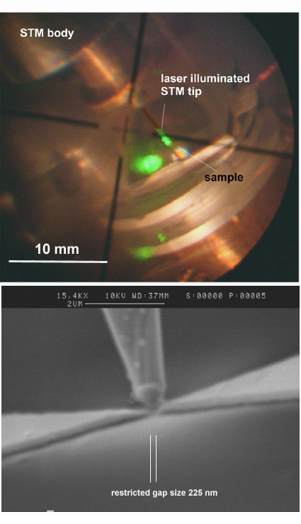
A scheme of the STM-SEM facility is reported below (left). The images on the right show an optical microscope view of the laser irradiated STM tip on the sample, and an SEM scan of the STM tip operating to deposit material on the tips of a couple of lithographic nanoelectrodes fabricated by A. Gerardino at the CNR-IFN electron beam facility.
This facility is particularly useful for precise positioning of the tip on the specific features or devices to be analyzed or operated upon. It allows STM electronic spectroscopy to be effected on features previously easily located on the basis of the difference in secondary electron emission. It allows a prompt characterization of both tip and sample surface damage. It supplies a first easy characterization of surface modifications, like nanometric pit formation or inorganic material depositions, when the sample is irradiated by laser beams. Finally it gives us the possibility to effect much shorter, and as a consequence slower and less damaging, STM scans for a complete characterization of the sample.
Related Information
contact: Dr. P. Morales
ENEA