

The Variable Temperature STM/AFM
Characteristics
Stainless steel UHV system (Standard pressure 6 10-11mbar).Turbo molecular pump for roughing: 240 l/sec – Ionic pump: 500 l/sec – Titanium sublimator.X-Y-Z manipulator with direct current or resistive heating. Tmax=1500 K.STM/AFM (piezoresistive).Heating at the STM position: up to 1500 K.Cooling at the STM position: down to 25 K.E-beam evaporators at the STM position: Ge and Si.Reverse view LEED-Auger with LaB6 filament.
Some Results
Ge/Si(111) – experiments performed were related to the visualization of the growth by Physical Vapour Deposition of Ge nanostructures on 7×7 Si(111) reconstructed surfaces. By evaporating Ge on Si(111) at T=500°C the formation ofwetting layers have been studied by Scanning Tunneling Microscopy in situ. The evolution of the Ge islands appearing after the wetting layer (completed at 3 ML). The 3D islands appear as truncated tetrahedrons (7×7 reconstructed on the top) and evolves into rounded shape, flat islands with a central hole. An erosion of the substrate around the islands has been also evidenced and measured. The island have lateral dimensions in the range 200 – 500 nm. The statistical distribution of the islands shapes and contact angles has been analysed. On Si step bunched surfaces (obtained by flashing at 1200°C in proper condition the Si substrate) the self aggregation and ordering of the islands has been evidenced. These results have been published in several papers and conference or school proceedings [1-6].
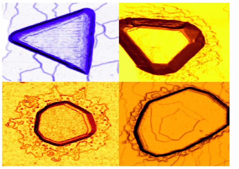
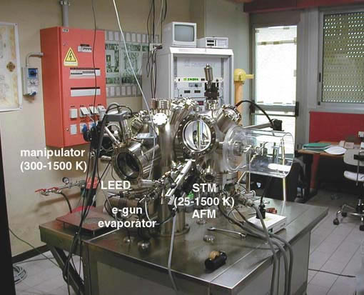
Fig 1. Ge islands grown on Si(111) observed by STM and AFM at various stages of evolution. Top left, a) an island after the nucleation (STM: 236x236x8 nm), top rigth, b) new facets (100 and 117) appear (STM: 230x230x38 nm); bottom left, c). First stage of ripening. (STM: 527x527x12 nm) bottom rigth, d) final stage of ripening (AFM image: 527x527x10 nm). Ge flux was 1 Å/min. The substrate temperature was 530 °C for a), 450 °C for b) and 500 °C for c) and d).
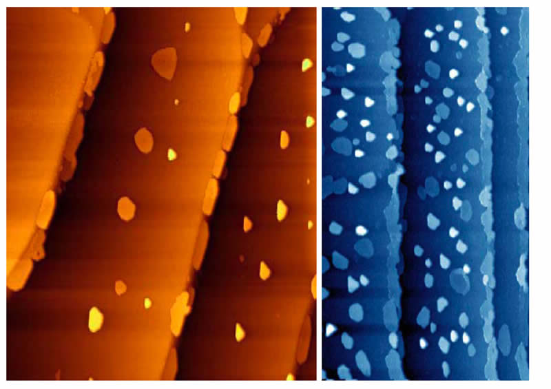
Fig 2. Organization of the Ge islands on a Si(111) step-bunched substrate a) STM image of 2.5 nm Ge deposition on Si(111) at T=450 °C 2.7×3.7 μm2. The total height of the image is 56 nm. b) STM image of 6 nm Ge deposition on Si(111) at T=450 °C 10×10 μm2. The total height of the image is 82 nm.InAs/GaAs quantum dotsThe InAs quantum dots on GaAs were prepared ex-situ by MBE as follows: the GaAs(001) wafer was initially deoxidized in As flux at 640 °C until a weak 2×4 RHEED pattern appeared. Afterwards, the substrate temperature was lowered to 590 °C and an epitaxial GaAs buffer layer of approximately 0.75 mm was grown at a rate of 1 μm/h. After 10 min of annealing, the temperature was further lowered to 500 °C for the InAs growth. The deposition rate was 0.028 ML/s with an In/As flux ratio of 1/15. The InAs coverage was 3 ML (the 2D-3D transition occurs at 1.6 ML). A 50 nm As capping layer is grown on top of the quantum dots, in order to protect the surface during the transfer to the AFM/STM chamber if atomic resolution and reconstruction have to be obtained by STM. The other samples are grown on intrinsic GaAs exhibiting a resistance too high to be imaged by STM, so the measurements are normally performed by AFM. Many samples, with different InAs coverages and growth modes have been prepared and measured. The size and distribution of the dots obtained in various growth conditions have been measured. Two main growth modes have been analysed: Continuous (the In flux was never interrupted) and Migration Enhanced (the In flux was interrupted at regular intervals, in order to increase the atomic movements ad aggregation on the surface). The island size increases in the Migration Enhanced mode. The onset of the quantum dot formation has been evidenced by also by STM, by imaging 2D islands after which act as precursors. The results have been published in two papers [7-8]
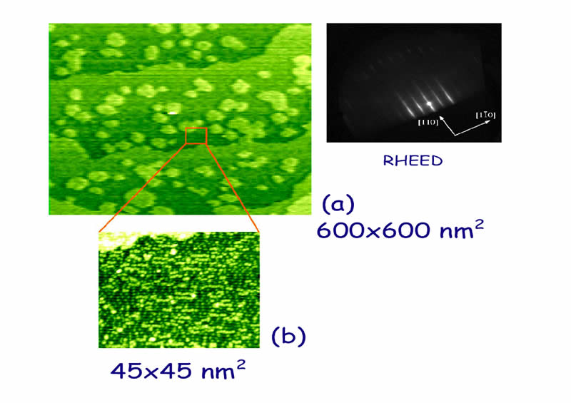 Fig 3. STM images at 1.3 ML of InAs on GaAs(001); a) 2D-islands of average height 0.4 nm (precursors); b) high resolution image of the wetting layer. The RHEED image has been acquired in the MBE system at the end of the growth.
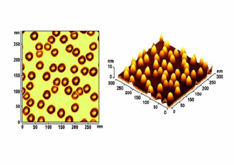 Fig 4. Needle-Sensor AFM of self-assembled quantum dots of InAs on GaAs(001) imaged using the VT SPM; dimensions: 300×300 nm. Height: 10 nm. The typical dot size is around 25 nm, and the height is 7 nm.
References on Ge/Si
[1] F. Boscherini, G. Capellini, L. Di Gaspare, F. Rosei, N. Motta and S. Mobilio, “Ge-Si intermixing in Ge quantum dots on Si(001) and Si(111)”, Appl. Phys. Lett. 76, 682 (2000).[2] F. Rosei, N. Motta, A. Sgarlata, G. Capellini and F. Boscherini, “Formation of the Wetting Layer in Ge/Si(111) studied by STM and XAFS”, Thin Solid Films 369 p29 (2000).[3] F. Boscherini, G. Capellini, L. Di Gaspare, F. Rosei, N. Motta and S. Mobilio, “Atomic intermixing in Ge Quantum Dots”,“ESRF Highlights” 1999, Surfaces and Interfaces (may be visualized on the web site www.esrf.fr).[4] F. Boscherini, G. Capellini, L. Di Gaspare, M. De Seta, F. Rosei, N. Motta A. Sgarlata and S. Mobilio, “Ge-Si intermixing in Ge quantum dots on Si”, Thin Solid Films 380, 173 (2000).[5] A. Sgarlata, F. Rosei, M. Fanfoni, N. Motta and A. Balzarotti, “STM/AFM study of Ge Quantum Dots grown on Si(111)”, IEEE Proceedings of the 11th International Semiconducting and Insulating Materials Conference, February 2000.[6] F. Rosei, N. Motta, A. Sgarlata and A. Balzarotti, “Growth and characterization of Ge nanostructures on Si(111)”, submitted for publication to Lecture Notes in Physics. (February 2001).[7] Nunzio Motta Self-assembled Quantum Dots studied by scanning probes and other structural techniques. Proc. Workshop on Nanotubes and Nanostructures 2000, S.M.Pula (CA), Ed. S.Bellucci, (Editrice Compositori 2001)[8] N. Motta, F. Rosei, A. Sgarlata, G. Capellini, S. Mobilio, F. Boscherini, Evolution of the intermixing process in Ge/Si(111) Self-assembled islands, submitted to Materials Science B
References on InAs/GaAs
[1] F. Patella, M. Fanfoni, F. Arciprete, S. Nufris, E. Placidi, and A. Balzarotti; Kinetic aspects of the morphology of self-assembled InAs quantum dots on GaAs(001) Applied Physics Letters 76 (2001) 320.[2] Arciprete, A. Balzarotti, M. Fanfoni, N. Motta, F. Patella, A. Sgarlata; Morphology of self-assembled quantum dots of InAs on GaAs(001) and Ge on Si(111) in Recent Research developments in Vacuum Science & Technology. Publisher: Transworld Research Network (2001).
Related Information
AFM contact: Prof. Massimo Fanfoni
STM contact: Prof. Anna Sgarlata